


Introduction 🔗
Hardware development tends to be more specialized, and compared to software engineers, there are fewer professionals in this field. The development process itself imposes various challenges, such as high manufacturing and development costs, scalability, reliability validation, intellectual property protection, et cetera. Despite these challenges, (experienced) professionals in hardware development will remain in high demand for many years to come, as many companies and individuals will continue to rely on existing technology, and engineers will remain crucial as hardware adapts and improves.
The hardware field is indeed expansive, with various solutions and architectures available for different challenges. In this series, we’ll concentrate on development specifically for FPGA (Field Programmable Gate Array) boards.
Does this sound intriguing to you? Are you ready to take on the challenge? Then follow me, as we together, explore the realm of hardware development.
What is an FPGA? 🔗
You are likely familiar with CPUs (Central Processing Units), the workhorses of modern computing. CPU's are hardware components that are general purpose and often excel in performance, essentially they are structured in a way that would allow firmware or operating system to utilize it in any way necessary to solve various (extensive) tasks. However, for solving a certain problem we might not need such a versatile or performance efficient hardware component. When looking at problem specific available options in the market, we arrive at couple alternatives - ASIC (Application Specific Integrated Circuit), MPSoC (Multi Processor System On Chip), FPGA (Field Programmable Gate Array). Note! If you are interested in the distinctive benefits each technology introduces, feel free to explore more, unfortunately it's out of scope for these series.
At this point you have been told that FPGAs are used to solve problem specific tasks. That indeed is quite vague, let's expand on that. First and foremost, the hardware structure of FPGAs greatly differs to that compared to a standard CPU. The basic architecture of an FPGA is made up of Configurable Logic Blocks (CLB's). Furthermore, these CLB's are made up of smaller components, such as Flip-Flops (memory units), Look-up Tables (containing hardwired outputs for every combination of inputs), Multiplexers. However, pay careful notice, we did NOT mention any logic gates (AND, OR, XOR, NOT, NAND, NOR and XNOR). As a matter of fact, that is correct, FPGA fabric contains no such basic gates, instead the required logic is performed by means of Look-up tables. An FPGA would contain hundreds or (usually) thousands of such CLB's, that when linked together solve complex logic functions.
Moreover, more expensive and advanced boards contain Hard IP's (Hard Intellectual Properties) - chip blocks that are etched into the silicon and perform a certain task very well (in a way better than the same solution made of CLB's). Some examples to mention: ARM CPU, Block RAM, et cetera.
FPGAs have a wide range of applications, they particularly excel in parallelism. To name few examples:
- High-performance computing: Accelerating scientific simulations, data analysis, and machine learning tasks.
- Image/audio processing: Accelerating image/audio processing, encoding or decoding.
- Embedded systems: Complex control units in industrial automation, aerospace.
Why Haskell & Clash? 🔗
These days, 'Hardware Description Language' (HDL), is used to write the great majority of hardware projects. These are declarative languages that let circuit designers explain how their designs behave. Although there are many HDLs available, Verilog and VHDL are the most widely used.
 This figure displays a simple implementation of an 'AND' gate in VHDL and Verilog, respectively.
I've included a short example of both of the descriptive languages above. I will not dive into too much detail, that would be beyond the scope of these series, for this there are plentiful of documentation and tutorials. Coming from a software development background, such HDL languages did not necessarily tickle my fancy.
Looking at alternatives, I came across a functional hardware description language - Clash. Clash is built upon the ideology of Haskell, from which both the syntax and semantics are borrowed. Functional properties of Clash, such as purity (no implied side effects, function output depends only on its input values, and no global state that could be altered), polymorphism, strict typing, and higher-order functions are the driving factors that enable developers to write concise and maintainable code both for combinational and sequential circuits.
How awesome is that?
Installation & Setup 🔗
There are couple tools we need to install to get started. The following steps will guide you to set everything up for a windows machine.
GHC & Cabal
GHC is a Haskell compiler, where as Cabal is a tool for building and packaging Haskell libraries and applications. The Haskell Downloads Page provides an installation guide, or GHCup which proposes a straight-forward and user friendly textual user interface. If you do decide to take the manual route, rather than utilizing GHCup, I can recommend the stable release version 9.8.2 for GHC, and 3.10.3.0 for Cabal.
Clash
Having completed the first step, proceed with clash installation.
Install clash-ghc by running the following command in CMD: cabal v1-install clash-ghc. Occasionally, this will require several runs of the installation command before everything compiles. Hence, if Cabal reports an error, check if the command continues past the error point by running it again. (Try cabal install clash-ghc, if the command v1-install is not present).
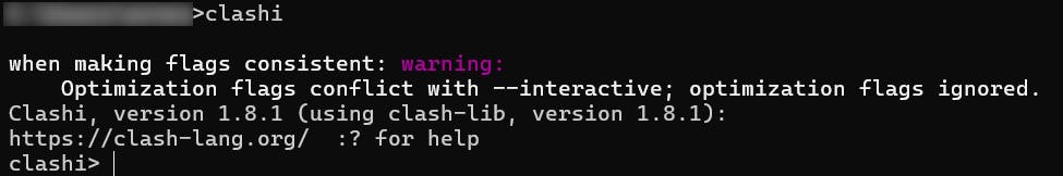
Validate that everything was successfully installed by entering clashi in CMD. You should be greeted with the clash interactive environment.
Xilinx Vivado
This tool is more demanding in terms of system requirements. It will come in handy in future series when we are going to be visualizing our circuit RTL (Register Transfer Language) schematics. For now, let's install it and set it aside for later use.
- To install the necessary software, you'll need to create an AMD account. You can sign up here: AMD Signup Page.
- Head to the downloads page: AMD Xilinx Vivado Download. The version of the software you want to download is 2024.1, namely the AMD Unified Installer for FPGAs & Adaptive SoCs 2024.1: Windows Self Extracting Web Installer.
- Follow the Setup Wizard (I have attached couple of images below to aid the installation process).
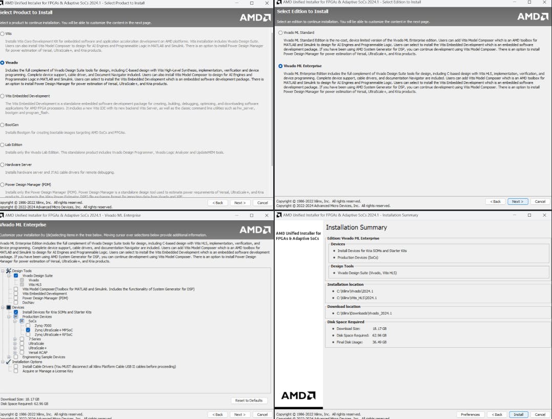
The final installation size is quite significant, at least 18GB. It is recommended to use stable and quick internet connection.
Wrapping up 🔗
The first section of the series is now complete. By talking about the particular difficulties in hardware development, we have set the foundation. Additionally, I briefly highlighted the vastness of the hardware field, emphasizing the upcoming focus on FPGA boards and the modern alternatives to traditional HDLs, particularly Clash, which leverages Haskells powerful functional programming paradigm.
We managed to also cover the essential setup steps, from installing GHC, Cabal and Clash to setting up Xilinx Vivado.
In the following series we will begin with a brief overview of Haskell, learn the fundamentals of Clash, and then work on implementing and analyzing various circuit designs.